My research mainly focuses on the following areas:
I. HEES System: Architecture, Configuration, Management, and Implementation back to top
Conventional EES systems only consist of a single type of EES element. Unfortunately, no available EES element can fulfill all the desired performance metrics of an ideal storage means, e.g., high power/energy density, low cost/weight per unit capacity, high round-trip efficiency, and long cycle life. An obvious shortcoming of a homogeneous EES system is that the key figures of merit (normalized with respect to capacity) of the system cannot be any better than those of its constituent EES element.
An HEES system is consisting of different types of EES elements (e.g., batteries and supercapacitors), where each type has its unique strengths and weaknesses. The HEES system can exploit the strength of each type of EES element and achieve a combination of performance metrics that is superior to that of any of its individual EES components. Based on the properties of the HEES system and characteristics of power sources (or load devices), we developed charge management policies (such as charge allocation, charge replacement, charge migration and bank re-configuration) to operate HEES system properly to achieve a near-optimal performance.
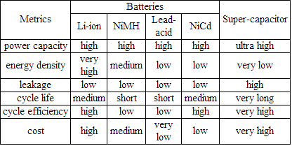
Properties of different EES elements (left) and the concept of the hybrid electrical energy storage system (right).
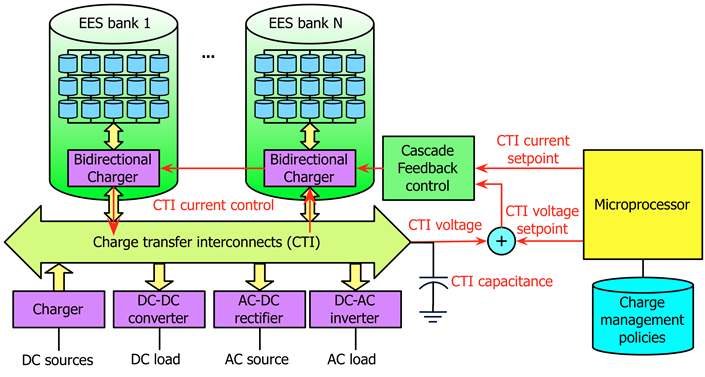
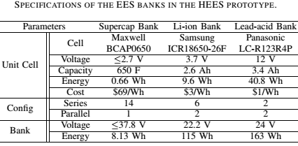
Block diagram (left) and the specifications of the HEES prototype (right).
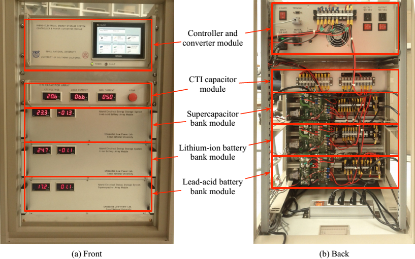
Picture of the HEES prototype (left) and the introduction video in HEES control implementaion (right).
I.1. Charge allocation
The charge allocation is to maximize the charge
allocation efficiency, defined as the ratio of energy
received by EES banks and the total energy provided by
power sources over a given time period, by properly
distributing power of the incoming power to selected
destination banks. We see to answer the following
questions: i) what is the optimal voltage level for the
charge transfer interconnect (CTI) , ii) among all the
possible destination EES banks, which one(s) should be
selected, and iii) among the selected destination EES
banks, how to allocate the charging currents to achieve
optimal global charge allocation efficiency for the
whole system over a given time period.
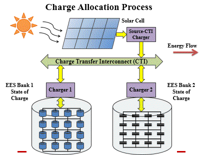
We formulate the global charge allocation (GCA) problemas an optimization problem. We start from solving the instantaneous charge allocation (ICA) problem, which seeks to optimize the charge allocation efficiency at a specific instance of time. Since the ICA problem is essentially a mixed integer non-linear optimization problem (MINLP), which is NP-complete, we propose an effective way of solving the ICA problem and get near-optimal solution in an iterative manner, where in each iteration we solve a convex optimization problem which can be solved in polynomial time. Near-optimal solutions of the original GCA problem can be obtained by incorporating time-dependent constraints for charging currents of different sets of EES banks in the ICA problem, and subsequently, solving the ICA problem with the imposed constraints at every decision epoch throughout the charge allocation process. Such constraints force the charge allocation manager to "consider the future energy production profile'', and thereby, avoid greedy decisions that may prove wrong e.g., over charging of certain (high efficiency) EES banks (such a scheme may result in efficiency degradation if some EES banks are already full.)
Related papers: CODES'11, TCAD'13.
I.2. Charge replacement
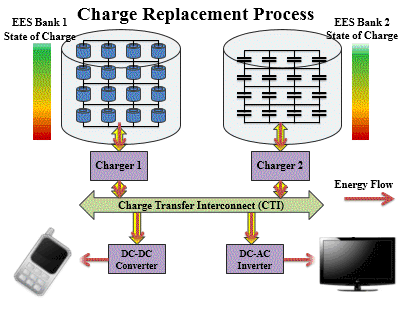 The charge replacement problem in the HEES system is to
adaptively select the EES banks and determine the
discharging currents, from zero to a maximum limit, and
the voltage level settings on a charge transfer
interconnect (CTI) so that the given load demand is met
and the charge replacement efficiency is maximized.
Unlike the charge allocation efficiency, charge
replacement efficiency denotes the ratio between the
energy requested by the load devices and the energy
retrieved from the HEES system. We provide a
mathematical formulation for the global charge
replacement (GCR) problem and propose an efficient
algorithm to solve it near-optimally. Precisely, the GCR
problem is formulated as an optimization problem where
the objective function is the GCR efficiency and
constraints are derived from laws of energy and charge
conservations. We account for the energy loss due to the
internal resistance of the batteries, the power
conversion inefficiencies, the rate capacity effect of
the batteries, and the self-discharge of the
supercapacitors. The GCR problem is solved using convex
optimization methods while imposing an output power
bound on the supercapacitor bank in order to avoid
discharging this bank too quickly (which would in turn
degrade the charge replacement efficiency).
The charge replacement problem in the HEES system is to
adaptively select the EES banks and determine the
discharging currents, from zero to a maximum limit, and
the voltage level settings on a charge transfer
interconnect (CTI) so that the given load demand is met
and the charge replacement efficiency is maximized.
Unlike the charge allocation efficiency, charge
replacement efficiency denotes the ratio between the
energy requested by the load devices and the energy
retrieved from the HEES system. We provide a
mathematical formulation for the global charge
replacement (GCR) problem and propose an efficient
algorithm to solve it near-optimally. Precisely, the GCR
problem is formulated as an optimization problem where
the objective function is the GCR efficiency and
constraints are derived from laws of energy and charge
conservations. We account for the energy loss due to the
internal resistance of the batteries, the power
conversion inefficiencies, the rate capacity effect of
the batteries, and the self-discharge of the
supercapacitors. The GCR problem is solved using convex
optimization methods while imposing an output power
bound on the supercapacitor bank in order to avoid
discharging this bank too quickly (which would in turn
degrade the charge replacement efficiency).
Related papers: ASPDAC'12.
I.3. Charge migration
While charge allocation and replacement deal with energy exchange with external power supply and load demand, charge migration is an internal energy transfer from one EES bank to another. We see strong motivations to perform charge migration to enhance the EES system performance. First, appropriate charge migration can improve the energy efficiency by controlling the SoC of the EES banks for future charge allocation or replacement. Second, we should not let a leaky EES bank, e.g., a supercapacitor bank, store charge for a long period of time. We had better perform charge migration from a supercapacitor bank to another if we foresee that the charge in the supercapacitor bank will not be replaced in the near future. Third, charge migration can maximize the availability of the EES system. An EES system cannot satisfy a load demand even if the total amount of charge in the EES system is enough for the load demand because of lack of power capacity.
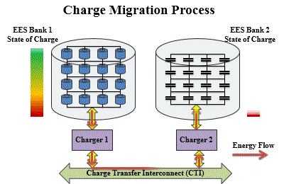 There
are different types of charge migration problems,
depending on how many source and destination banks there
are and the number of available CTIs. The single-source,
single-destination (SSSD) migration utilizes a single
CTI during the whole migration process. The simultaneous
multiple-source, multiple-destination (MSMD) migrations
can significantly speed up the whole migration process
and can improve the overall charge migration efficiency.
The charge migration scheduling (CMS) problem is much
more general. It enables a number of concurrent MSMD
charge migrations through a fixed number of CTIs while
meeting a global deadline constraint. The objective is
to maximize the overall charge migration efficiency (by
minimizing the charge that is extracted from the source
banks since the charge that is delivered to the
destinations banks is specified as part of the problem
statement.)
There
are different types of charge migration problems,
depending on how many source and destination banks there
are and the number of available CTIs. The single-source,
single-destination (SSSD) migration utilizes a single
CTI during the whole migration process. The simultaneous
multiple-source, multiple-destination (MSMD) migrations
can significantly speed up the whole migration process
and can improve the overall charge migration efficiency.
The charge migration scheduling (CMS) problem is much
more general. It enables a number of concurrent MSMD
charge migrations through a fixed number of CTIs while
meeting a global deadline constraint. The objective is
to maximize the overall charge migration efficiency (by
minimizing the charge that is extracted from the source
banks since the charge that is delivered to the
destinations banks is specified as part of the problem
statement.)
Related papers: ISLPED'11, DATE'12, ASPDAC'13.
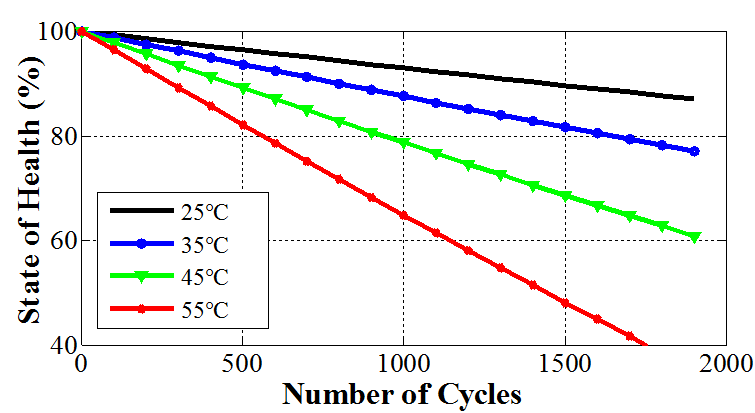
I.4. State-of-health-aware charge management
The cycle life of the EES elements is one of the most
important metrics that should be considered by the
designers of the EES system. State of health-aware
charge management problem in HEES systems is to find
charging/discharging current profiles for all EES banks
and CTI voltage, aiming to improve both the cycle life
of the EES arrays (mainly battery arrays) and overall
cycle efficiency of the entire system. The system
lifetime is usually described using the state of health
(SoH), which is defined as the ratio of full charge
capacity of a cycle-aged EES element to its designed
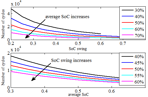
capacity. We determine the SoH degradation rate with
respect to different average state of charges (SoCs),
and SoC swings (defined as SoC change during a charging
/ discharging cycle). The right figure shows that more
severe SoH degradation is caused by 1) greater SoC swing
per cycle and 2) larger average SoC level in each cycle.
In HEES systems, battery arrays have higher energy capacity but relatively lower cycle life and cycle efficiency. We use the supercapacitor arrays as buffer of battery arrays because it has strengths of high power capacity, superior cycle efficiency and long cycle life but weakness of low energy capacity. We maintain the desired charging current of the battery banks in charging process, allowing the supercapacitor banks to accept the extra power from CTI or supply power to battery banks. Similar strategy is also used during the discharging process, we let the supercapacitor banks compensate power shortage caused by high load demand and get charged from battery banks to maintain their SoC when the load demand is low.
Related papers: DATE'12.
II. Thermal Simulation, Management, and Design Optimization in Embedded Systems back to top
II.1 Therminator: A Thermal Simulator for Smartphones
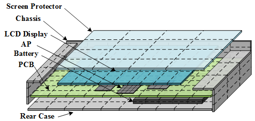
Thermal design and management of smartphones is concerned with a new challenge: the constraint of skin temperature. This constraint refers to the fact that the temperature at the device skin must not exceed a certain upper threshold. Reference showed that most people experience a sensation of heat pain when they touch an object hotter than 45˚C. Ideally speaking, distributing the heat uniformly onto the device skin results in the most effective heat dissipation. However, in practice, majority of the heat flows in vertical direction from the AP die, and thus hot spots with a high temperature are formed on the device skin.
To address this design challenge, we designed Therminator, a compact thermal modeling-based component-level thermal simulator targeting at small form-factor mobile devices (such as smartphones). It produces temperature maps for all components, including the AP, battery, display, and other key device components, as well as the skin of the device itself, with high accuracy and fast runtime. Therminator results have been validated against thermocouple measurements on multiple devices and simulation results generated by Autodesk Simulation CFD. In addition, Therminator is very versatile in the sense of handling different device specifications and component usage information, which allows a user to explore impacts of different thermal designs and thermal management policies. New devices can be simply described through an input file (in XML format). Finally, Therminator has implemented a parallel processing feature, allowing users to use GPU to reduce the runtime by more than two orders of magnitude for high-resolution temperature maps.
Therminator takes two input files provided by users. The specs.xml file describes the smartphone design, including components of interest and their geometric dimensions (length, width, and thickness) and relative positions. Therminator has a built-in library storing properties of common material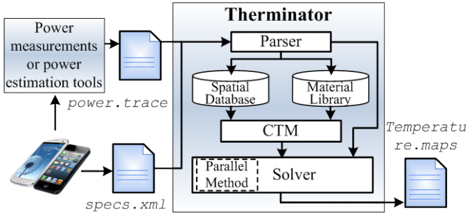 s (i.e., thermal conductivity, density, and specific heat) that are used to manufacture smartphones. In addition, users can override these properties or specify new materials through the specs.xml file. The power.trace file provides the usage information (power consumption) of those components that consume power and generate heat, e.g., ICs, battery, and display. The power.trace can be obtained through real measurements or other power estimation tools/methods. power.trace is a separate file so that one can easily interface a performance-power simulator with Therminator.
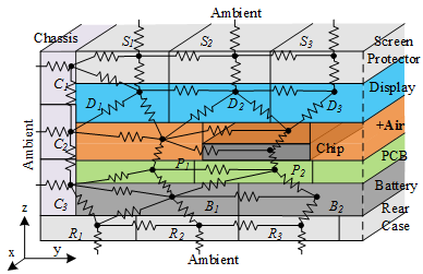
Thermal resistance network in compact modeling (left) and the Qualcomm MDP device for Therminator (right).
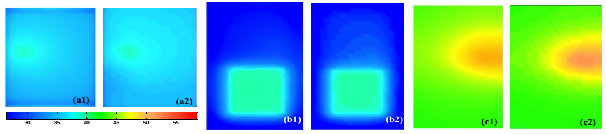
Temperature maps produced by Autodesk Simulation CFD (a1, b1, c1) and by Therminator (a2, b2, c2) for the screen protector (a), rear case (b), and PCB (c) for StabilityTest usecase.
Related papers: ISLPED'14.
II.2. Thermal coupling effect in smartphones
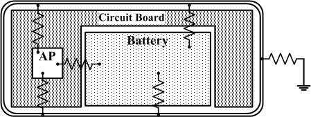 The
thermal management is a crucial design problem for
mobile devices because it greatly affects not only the
device reliability, but also the leakage energy
consumption. Conventional dynamic thermal management
(DTM) techniques work well for the computer systems.
However, due to the limitation of the physical space in
mobile devices, the thermal coupling effect between the
major heat generation components, such as the
application processor (AP) and the battery, plays an
important role in determining the temperature inside the
mobile device package.
The
thermal management is a crucial design problem for
mobile devices because it greatly affects not only the
device reliability, but also the leakage energy
consumption. Conventional dynamic thermal management
(DTM) techniques work well for the computer systems.
However, due to the limitation of the physical space in
mobile devices, the thermal coupling effect between the
major heat generation components, such as the
application processor (AP) and the battery, plays an
important role in determining the temperature inside the
mobile device package.
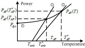 Due
to this effect, the thermal behavior of one part is no
longer independent of the other, but is affected by the
temperature of other parts. In particular, we build the
thermal RC-circuit model to account for this effect and
provides a quantitative characterization process to
extract corresponding parameters through practical
experiments. We also present a DTM method combining the
thermal sensor readouts, look-up tables (LUTs), and the
RC-circuit thermal modeling. For each task, we calculate
the minimum frequency that guarantees to meet deadline
constraints and lookup the maximum frequency that avoids
thermal violations from pre-characterized tables. The
DTM policy is based on the relationship between these
two frequencies. In case of a thermal violation is
predicted, a DTM response mechanism is activated, e.g.,
reducing the operating frequency or dropping the task,
to avoid the potential violation of the critical
temperature.
Due
to this effect, the thermal behavior of one part is no
longer independent of the other, but is affected by the
temperature of other parts. In particular, we build the
thermal RC-circuit model to account for this effect and
provides a quantitative characterization process to
extract corresponding parameters through practical
experiments. We also present a DTM method combining the
thermal sensor readouts, look-up tables (LUTs), and the
RC-circuit thermal modeling. For each task, we calculate
the minimum frequency that guarantees to meet deadline
constraints and lookup the maximum frequency that avoids
thermal violations from pre-characterized tables. The
DTM policy is based on the relationship between these
two frequencies. In case of a thermal violation is
predicted, a DTM response mechanism is activated, e.g.,
reducing the operating frequency or dropping the task,
to avoid the potential violation of the critical
temperature.
Related papers: ICCAD'13.
II.3. Battery cooling to extend the service lifetime
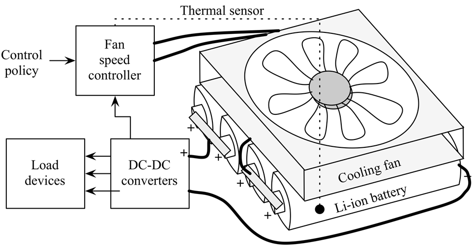 Cycle
life of a battery largely varies according to the
battery operating conditions, especially the battery
temperature. In particular, batteries age much faster at
high temperature. Extensive experiments have shown that
the battery temperature varies dramatically during
continuous charge or discharge process. Therefore, we
explore the opportunity to use properly designed and
controlled forced convection cooling such as cooling fan
and develops corresponding thermal management policy, in
order to control the battery temperature, and thereby
improve cycle life of the batteries in portable systems.
There is a fundamental tradeoff between the service time
of a battery equipped with fans and the cycle life of
the same battery. In particular, as the fan speed is
increased, the power dissipated by the fan goes up and
hence the full charge capacity of the battery is lost at
a faster rate, but at the same time, the battery
temperature remains lower and hence the battery
longevity increases.
Cycle
life of a battery largely varies according to the
battery operating conditions, especially the battery
temperature. In particular, batteries age much faster at
high temperature. Extensive experiments have shown that
the battery temperature varies dramatically during
continuous charge or discharge process. Therefore, we
explore the opportunity to use properly designed and
controlled forced convection cooling such as cooling fan
and develops corresponding thermal management policy, in
order to control the battery temperature, and thereby
improve cycle life of the batteries in portable systems.
There is a fundamental tradeoff between the service time
of a battery equipped with fans and the cycle life of
the same battery. In particular, as the fan speed is
increased, the power dissipated by the fan goes up and
hence the full charge capacity of the battery is lost at
a faster rate, but at the same time, the battery
temperature remains lower and hence the battery
longevity increases.
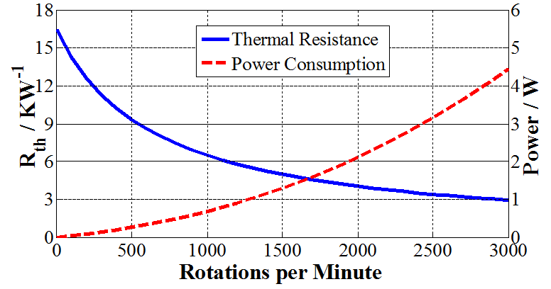
SoH degradation versus cycle life at different battery temperature (left) and the trade-off of fan usage (right).
Related papers: DATE'13.
III. Low Power Design in VLSI Circuits back to top
III.1. 7nm FinFET Standard Cell Libraries
A standard cell library containing timing and power information at different input and output conditions, i.e., input slew rates and output load capacitance, is required to enable logic synthesis, time and power analysis with advanced FinFET device technology nodes. We generate 7nm FinFET device models by using Synopsys TCAD simulator and characterize standard cells through HSPICE simulations. Multiple supply voltages ranging from the near-threshold to the super-threshold regime are supported in our 7nm FinFET technology nodes, allowing both high performance and low power usage. In addition, devices with multiple threshold voltages are supported to enable multi-threshold technology. Synthesis results demonstrate that 7nm FinFET technology can achieve 15X circuit speed improvement and 350X energy consumption reduction, against the 45nm CMOS technology.
Minimal energy point (left) and the minimal energy-delay-product point (right) of a 20-stage inverter synthesized using 7nm FinFET cell library.
Energy and delay values of a 16-bit adder (left) and dynamic/leakage power consumption of c432 (right) for different standard cell libraries.
III.2. An efficiecnt HCI effect simulation flow
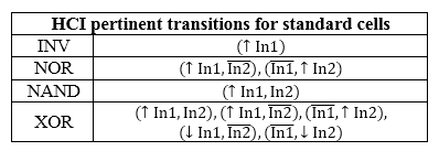 Hot
carrier injection (HCI) effect, which causes MOSFET
aging due to the deleterious effect on threshold voltage
and the driving current, becomes one of the major
concerns on the reliability degradation. An accurate and
efficient simulator with the HCI effect modeling
methodology is therefore crucial for predicting the
circuit performance and reliability and hinting the
circuit design and manufacturing. We present a
reliability simulation flow with fast run time and high
accuracy. To characterize the HCI effect of a
transistor, we propose an efficient HCI modeling method
based on piecewise linear curving fitting and HSpice
simulation. At the gate level, we propose two pruning
techniques to reduce the effort of standard cell library
characterization, based on the HCI effect dependency on
the input slew rate, load capacitance, rise/fall/steady
type of input transitions, and total transition counts.
Then we introduce the concept of pertinent transition,
which is the combination of input transition that does
causes HCI-induced aging in a logic cell. Additionally,
at the full chip level, to further improve the run time,
we classify all logic cells in the benchmark circuits
into two categories: critical and non-critical. We apply
different time step granularity to save the simulation
workload as well as maintain the accuracy.
Hot
carrier injection (HCI) effect, which causes MOSFET
aging due to the deleterious effect on threshold voltage
and the driving current, becomes one of the major
concerns on the reliability degradation. An accurate and
efficient simulator with the HCI effect modeling
methodology is therefore crucial for predicting the
circuit performance and reliability and hinting the
circuit design and manufacturing. We present a
reliability simulation flow with fast run time and high
accuracy. To characterize the HCI effect of a
transistor, we propose an efficient HCI modeling method
based on piecewise linear curving fitting and HSpice
simulation. At the gate level, we propose two pruning
techniques to reduce the effort of standard cell library
characterization, based on the HCI effect dependency on
the input slew rate, load capacitance, rise/fall/steady
type of input transitions, and total transition counts.
Then we introduce the concept of pertinent transition,
which is the combination of input transition that does
causes HCI-induced aging in a logic cell. Additionally,
at the full chip level, to further improve the run time,
we classify all logic cells in the benchmark circuits
into two categories: critical and non-critical. We apply
different time step granularity to save the simulation
workload as well as maintain the accuracy.
Related papers: ICCD'12.
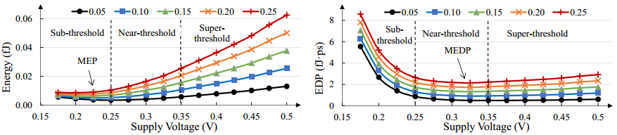
III.3. Soft-edge pipeline design in near-threshold voltage regime
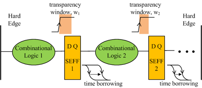 Near-threshold
(NT) operation, is quite effective in minimizing the
energy consumption of a design by reducing its supply
voltage to a level close to the threshold voltage of the
transistors, Vth. However,
digital circuits operating in the NT regime become quite
sensitive to process-induced variations.
Soft-edge flip-flop (SEFF) based pipelines can improve
the performance and energy efficiency of circuits
operating in the super-threshold
Near-threshold
(NT) operation, is quite effective in minimizing the
energy consumption of a design by reducing its supply
voltage to a level close to the threshold voltage of the
transistors, Vth. However,
digital circuits operating in the NT regime become quite
sensitive to process-induced variations.
Soft-edge flip-flop (SEFF) based pipelines can improve
the performance and energy efficiency of circuits
operating in the super-threshold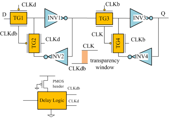 (supply voltage) regime by allowing opportunistic time
borrowing. The application of this technique to the
near-threshold regime of operation, however, faces a
significant challenge due to large circuit parameter
variations that result from manufacturing process
imperfections.
(supply voltage) regime by allowing opportunistic time
borrowing. The application of this technique to the
near-threshold regime of operation, however, faces a
significant challenge due to large circuit parameter
variations that result from manufacturing process
imperfections.
We focus on designing and optimizing SEFF-based linear pipelines that can operate in multiple supply voltages regimes. In order to design the SEFF-based pipeline circuits that can operate in all supply voltage regimes, we add a PMOS header on top of the conventional DL (beneath the supply voltage rail). The header PMOS results in a slight supply voltage drop on the DL, which is negligible in the ST regime but has a significant impact on the softness in the NT regime. We formulate the SEFF-based linear pipeline design problems and determine the optimal operating conditions, including the supply voltage and operating frequency, according to the problem setup and pipeline designs.
We solve two types of SEFF-based linear pipeline design problems. The first problem setup targets the general use of pipeline circuits i.e., enabling them to operate in all voltage regimes. We adopt the energy-delay product (EDP) as the cost function and minimize it over all supply voltage levels. We construct Pareto-optimal tradeoff curves of the DL between energy/power consumptions and FF softness so that we can select the DL configuration and sizing solution that are closest to the optimal ones. The second problem targets the situation in which the target pipeline circuit is required to meet some pre-specified minimum operating frequency. We adopt the total energy consumption per clock cycle as the cost function to minimize,as the frequency is constrained by the problem setup. We find the MEP and corresponding pipeline design parameters that satisfy the frequency constraints.
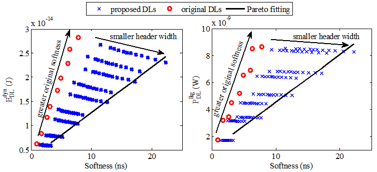
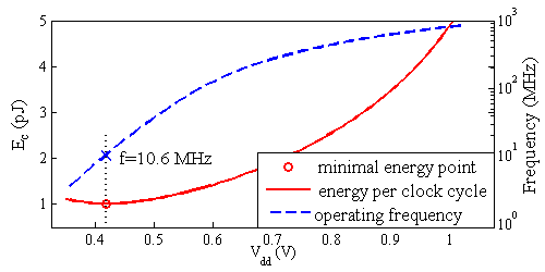
Pareto-optimal curves of DL energy/power consumptions and softness (left) and the minimal-energy-point (right).
Related papers: GLSVLSI'13.
IV. System Level Dynamic Power Management back to top
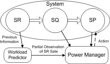 Dynamic
power management (DPM), defined as the selective shut-off
or slow-down of system components that are idle or
underutilized, has proven to be an effective technique for
reducing power dissipation at system level. An effective DPM
policy should minimize power consumption while maintaining
performance degradation to an acceptable level. Design of such
DPM policies has been an active research area. We presented an
online and model-free DPM technique based on reinforcement
learning.
Dynamic
power management (DPM), defined as the selective shut-off
or slow-down of system components that are idle or
underutilized, has proven to be an effective technique for
reducing power dissipation at system level. An effective DPM
policy should minimize power consumption while maintaining
performance degradation to an acceptable level. Design of such
DPM policies has been an active research area. We presented an
online and model-free DPM technique based on reinforcement
learning.
Related papers: DAC'11.
Previous Research Projects back to top
Regulation of Ionic Currents in Ventricular Myocytes
The expression levels of ionic currents in ventricular myocytes could vary largely at different genetic, pathological and pharmacological circumstances. Under the supervision of Prof. Alain Karma, we did research on the relation of expression levels of ionic currents and behaviors of myocytes. We explained the mechanism of ionic currents regulation and found the regulation ability quantitatively.
Fermion Gas in BCS-BEC Crossover
Under the supervision of Prof. Yongli Ma, we did research about ground state properties of a trapped Fermi gas. Using Thomas-Fermi approximation, we solved Gross-Pitaevskii equation, and found the ground state solution of the superfluid trapped fermion condensed states in BCS-BEC crossover.